


NEWS
Chemical Vapor Deposition, CVD is one of the key processes in semiconductor manufacturing, which generates solid thin films through chemical reactions of gas-phase reactants and deposits them on the substrate surface. So what are the applications of CVD in the semiconductor field?
1. Thin film deposition
Insulation layer deposition: CVD is used to deposit insulation layers such as silicon dioxide (SiO ₂) and silicon nitride (Si ₂ N ₄), playing a role in electrical insulation, protection, and passivation.
Metal layer deposition: The deposition of metal layers such as tungsten (W), titanium (Ti), titanium nitride (TiN), and aluminum (Al) for interconnection and contact hole filling.
Doping layer deposition: such as phosphorosilicate glass (PSG) and borosilicate glass (BSG), used for local doping and surface passivation.
2. Crystal growth
Epitaxial growth: CVD is used for epitaxial growth of monocrystalline silicon or other semiconductor materials (such as silicon carbide and gallium nitride), forming high-quality single crystal layers on the surface of the wafer.
Carbon nanotube and graphene growth: used for growing carbon nanotube and graphene materials, which are widely used in electronic devices and sensors.
3. High k dielectric
High k material deposition: High k dielectric materials such as hafnium oxide (HfO ₂) and zirconium oxide (ZrO ₂) are used as gate dielectrics in MOSFETs to reduce leakage current and improve device performance.
4. Barrier layer and lining layer
Barrier layer deposition: such as titanium nitride (TiN) and tantalum nitride (TaN), act as diffusion barriers for copper interconnects to prevent metal diffusion.
Backing layer deposition: used to improve interface quality, improve the uniformity and adhesion of subsequent film deposition.
5. Hard Mask in Photolithography Process
Hard mask layer deposition: such as silicon nitride (Si ₂ N ₄) and silicon oxide (SiO ₂), used as hard masks in lithography processes to provide high-resolution pattern transfer and etching protection.
")
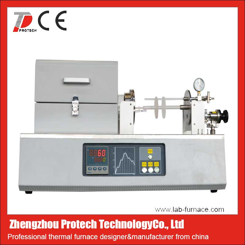
Second temperature zone vacuum CVD furnace (click on the image to view product details)
6. Optoelectronic device manufacturing
Photovoltaic cells: CVD is used to manufacture thin film solar cells, such as silicon thin films and compound semiconductor thin films (such as CdTe and CIGS), to improve photovoltaic conversion efficiency.
LED and Laser: Used for depositing gallium nitride (GaN) and other III-V compound semiconductors, manufacturing efficient light-emitting diodes (LEDs) and lasers.
7. Sensors and MEMS
Micro Electro Mechanical Systems (MEMS): CVD is used for depositing materials such as polycrystalline silicon and silicon oxide, manufacturing micro mechanical structures and sensors.
Gas sensors, such as metal oxide semiconductor gas sensors, achieve high sensitivity detection by depositing sensitive films through CVD.
8. Advanced packaging
Through Silicon Through Holes (TSV): CVD is used to deposit high-quality insulation layers and metal filling materials, and to manufacture three-dimensional integrated circuits (3D ICs) interconnection through TSV.
Packaging protective layer: used for depositing protective layers to improve packaging reliability and durability.
")
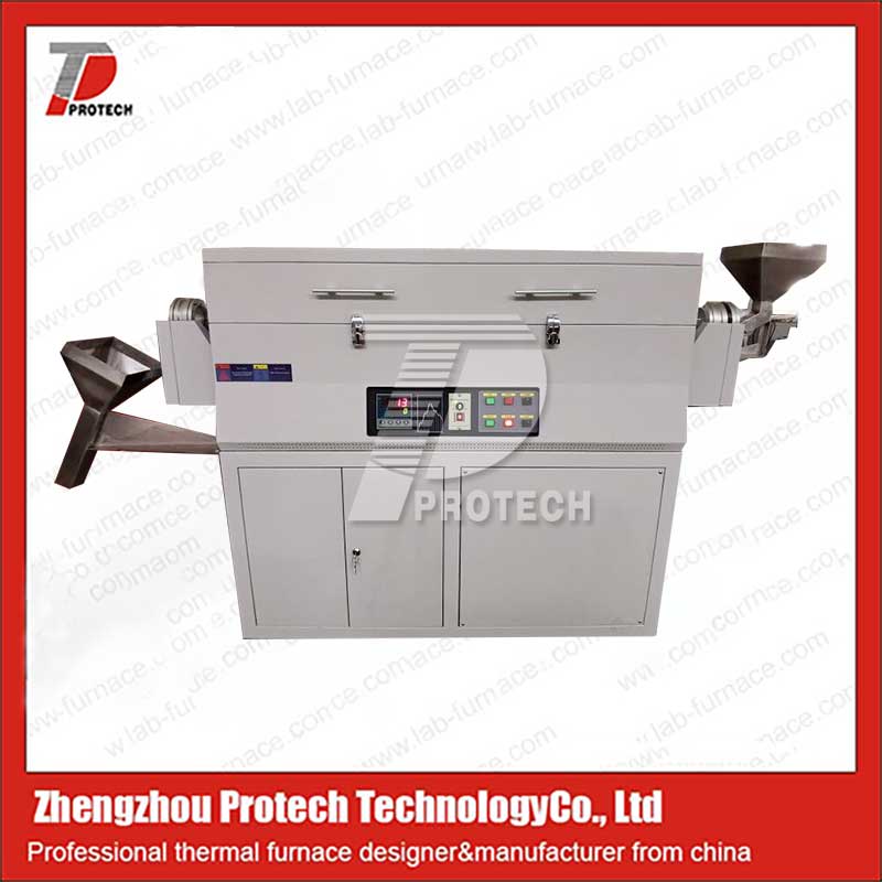
Three temperature zone CVD furnace (click on the image to view product details)
What are the advantages of CVD's application in the semiconductor field?
High purity and quality: The CVD process can deposit thin films with high purity and low defects, ensuring device performance and reliability.
Uniformity and controllability: By precisely controlling the flow rate and reaction conditions of gas-phase reactants, the thickness and composition uniformity of the film can be achieved.
Compatibility and diversity: The CVD process is suitable for a variety of materials and substrates, and is widely used in different semiconductor manufacturing steps.
The widespread application and multifaceted advantages of CVD in semiconductor manufacturing have made it a widely used process technology, leading to continuous progress and innovation in semiconductor devices.Click to learn more CVD devices! Or click on online customer service to learn more about product information!
Leave A Message
")


