


NEWS
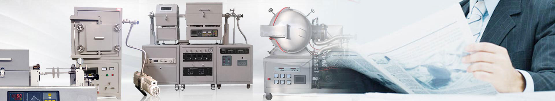
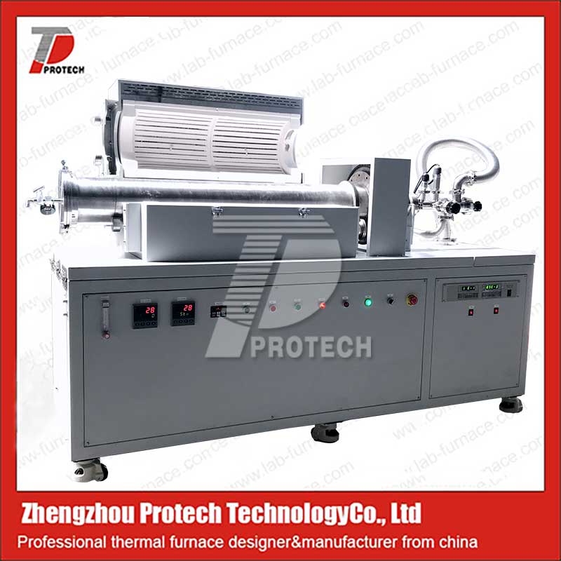
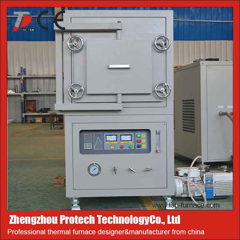
The vacuum tube CVD electric furnace (chemical vapor deposition electric furnace) has shown wide application value in materials science, electronics industry, energy, environmental protection, and manufacturing fields due to its precise control ability under high temperature, vacuum, or atmosphere protection environment. Let's take a detailed look below!
")
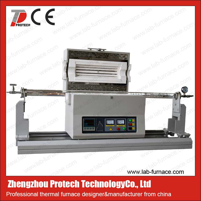
A commonly used 1100 ℃ vacuum tube CVD electric furnace (click on the image to view product details)
1. Material preparation and thin film deposition
Thin film material synthesis: Metal thin films (such as tungsten and aluminum), semiconductor thin films (such as silicon and silicon carbide), optical thin films (such as silicon nitride and silicon oxide), etc. can be prepared by decomposing and depositing gas-phase precursors on the substrate surface at high temperatures. These thin films play a significant role in electronic devices such as integrated circuits and sensors, optical coatings such as anti reflective and anti reflective films, and protective coatings such as wear-resistant and corrosion-resistant coatings.
Nanomaterial preparation: By adjusting reaction conditions such as temperature, gas flow rate, and pressure, structures such as nanoparticles, nanowires, and nanosheets can be synthesized. For example, the growth of carbon nanotubes and graphene relies on CVD technology, which has enormous potential in the fields of flexible electronics, energy storage devices, and sensors.
Ceramic and glass manufacturing: used for powder roasting and sintering of ceramic materials to increase material density and hardness; During the process of glass melting, a vacuum environment can reduce the generation of bubbles and improve optical transparency.
2. Electronics and Semiconductor Industry
Integrated circuit manufacturing: CVD is the core technology for depositing insulation layers (such as silicon dioxide and silicon nitride), metal interconnect layers (such as tungsten and copper), and doping layers (such as phosphosilicate glass). For example, the deposition of high-k dielectric materials such as hafnium oxide can reduce MOSFET gate leakage current and improve device performance.
Epitaxial growth: Growing high-quality single crystal layers on the surface of single crystal silicon or other semiconductor materials (such as gallium nitride and silicon carbide) for manufacturing high-performance power devices and optoelectronic devices. The silicon carbide CVD furnace has achieved mass production of 8-inch wafers, driving a 50% reduction in chip costs.
Micro Electro Mechanical Systems (MEMS): Deposition of polycrystalline silicon, silicon oxide and other materials to manufacture micro mechanical structures and sensors, such as accelerometers, pressure sensors, etc.
3. Energy sector
Photovoltaic cells: CVD is used to prepare silicon thin film solar cells and compound semiconductor thin films (such as CdTe, CIGS) to improve photoelectric conversion efficiency. For example, silicon-based thin-film cells achieve low-cost and flexible design by depositing amorphous or microcrystalline silicon layers through CVD.
Clean energy production: In biomass energy conversion, CVD furnaces can convert organic waste into synthesis gas (CO+H ₂) through high-temperature pyrolysis, providing raw materials for fuel cells.
4. Manufacturing and Protection
Aerospace: CVD silicon carbide coating can resist high-temperature airflow erosion at 3000 ℃, applied to rocket engine nozzles and hypersonic aircraft surfaces, with a lifespan increase of more than 5 times.
In the field of nuclear energy, SiC coated fuel particles can lock in radioactive substances for a long time, ensuring the safe operation of nuclear reactors.
The automotive industry adopts silicon carbide inverters, which improve charging efficiency and increase range. CVD technology is widely used in the field of new energy.
5. Environmental Protection and Resource Utilization
Waste disposal: Through high-temperature incineration or pyrolysis, CVD furnaces can achieve harmless treatment of waste plastics and electronic waste, and recover valuable substances such as precious metals.
Gas sensors: Deposition of metal oxide semiconductor sensitive thin films (such as SnO ₂ ZnO), Realize high-sensitivity detection of toxic gases (such as CO, NO ₂) for environmental monitoring and industrial safety applications.
6. Research and experimental platform
Materials research: Researchers use CVD furnaces to study the thermal stability, phase transition behavior, and chemical reaction mechanisms of materials, providing data support for the development of new materials.
High temperature experiment: supports complex experiments such as atmosphere reduction and vacuum annealing, simulates material properties under extreme environments, and is beneficial for exploring the forefront of materials science.
Technological advantages support application expansion
Precise control: equipped with a Mass Flow Controller (MFC), ensuring stable gas flow and uniformity of the film; 30 segment program temperature control intelligent PID regulation, achieving automatic heating/cooling.
Efficient and energy-saving: The double-layer furnace shell is designed with forced air cooling, with a surface temperature of ≤ 45 ℃. When the furnace is heated to 1100 ℃, the power consumption is low, and the cost of a single experiment is reduced.
Safe and reliable: The safety lock system includes over temperature protection, thermocouple protection, leakage protection, and door opening to cut off heating, ensuring the safety of operators and equipment.
Future Trends
With the development of fields such as 5G communication, quantum computing, and deep space exploration, CVD technology is breaking through towards the preparation of large-sized single crystals (such as 8-inch silicon carbide wafers), heterogeneous integration (SiC combined with gallium nitride), and green processes (zero toxic emissions), further expanding its application boundaries in new material manufacturing and sustainable development.Click to learn more CVD devices! Or click on online customer service to learn more about product information!
Leave A Message
")


