
 English
 简体中文
简体中文 French
 日本語
日本語 Korean
 Português
 Русский
 Spanish



NEWS
PECVD plasma enhanced chemical vapor deposition is the core process for preparing various insulation films, passivation films, and dielectric films in semiconductor wafer manufacturing, chip packaging, and micro/nano device processing. Compared with traditional LPCVD low-pressure chemical vapor deposition and APCVD atmospheric pressure chemical vapor deposition technologies, PECVD treatment of semiconductor thin films has multiple core advantages such as low-temperature deposition, good film uniformity, high deposition rate, and wide adaptability. It is currently the mainstream process for batch preparation of semiconductor thin films. Below is a detailed breakdown of the core advantages, process characteristics, and industry application scenarios of PECVD processing of semiconductor thin films.

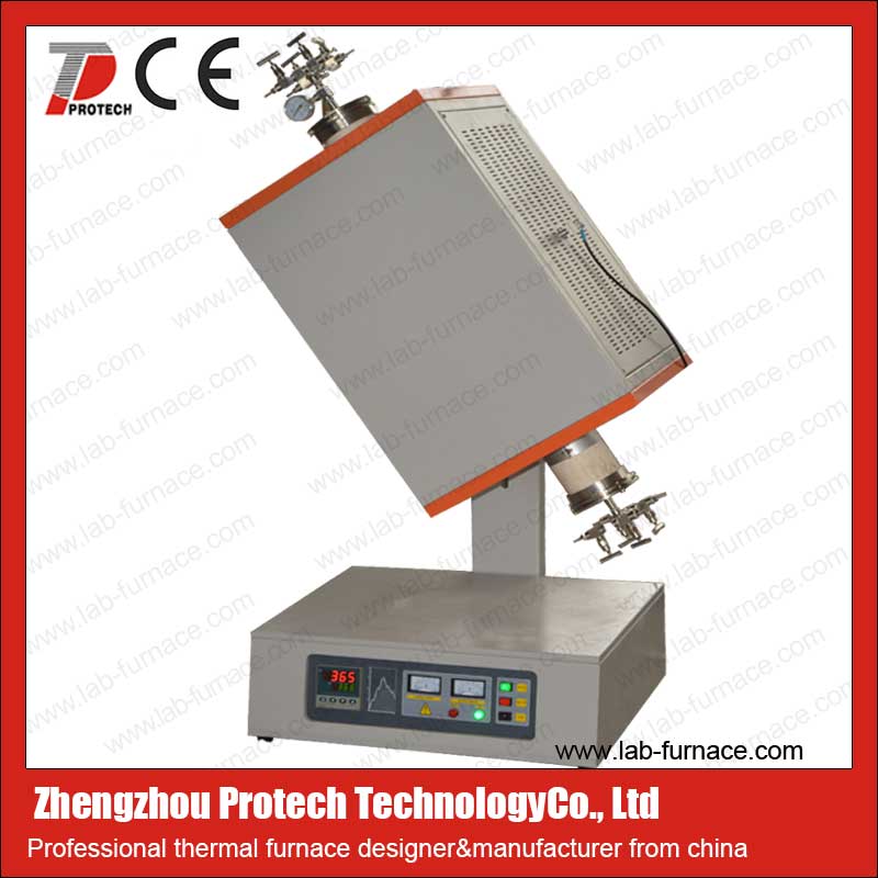
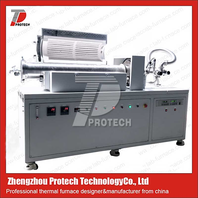
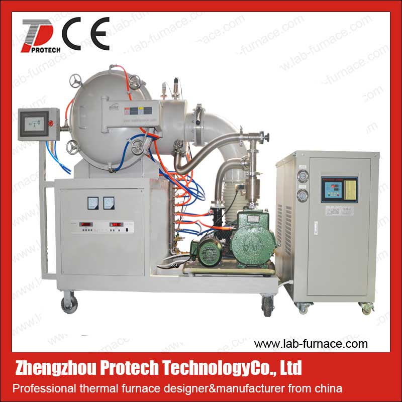
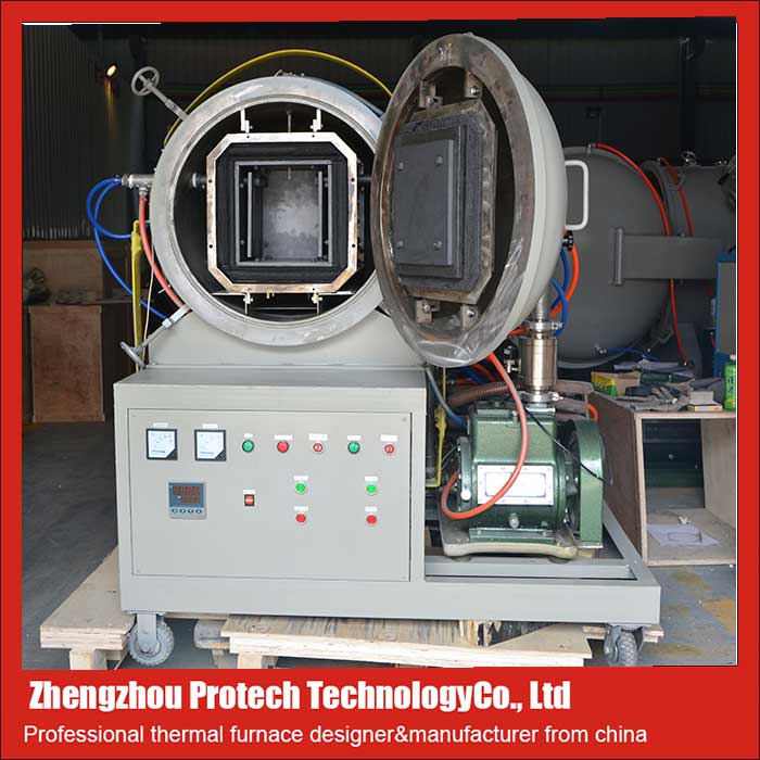
Commonly used PECVD electric furnaces (click on the image to view product details)
1. Core advantage: Low temperature deposition, no damage to semiconductor substrate
The traditional CVD process requires a high temperature environment (above 700 ℃) to complete thin film deposition, which can easily lead to thermal stress deformation, doping element diffusion, metal layer failure, and other problems in semiconductor wafers and chip substrates, seriously affecting device performance.
The biggest core advantage of PECVD is the low-temperature process, which relies on the plasma electric field to activate the reaction gas. Gas molecules can be cracked without high temperature heating, and thin film deposition can be completed in the low-temperature range of 200 ℃ -400 ℃. Low temperature processing throughout the process will not damage the crystal structure, metal wiring, and doping accuracy of semiconductor wafers, better adapting to the thin film preparation needs of CMOS chips, MEMS microdevices, flexible semiconductor materials, and precision wafers, effectively eliminating the potential for device failure caused by high temperatures.
2. Good film uniformity, suitable for high-precision semiconductor processes
Semiconductor devices require high uniformity in film thickness, density, and refractive index. Uneven film thickness and local density differences can directly lead to chip leakage, insufficient voltage resistance, and decreased device yield.
PECVD equipment uniformly excites the plasma inside the cavity through radio frequency electric field, and with better pressure, airflow, and temperature control system, can form a thin film layer with uniform thickness, dense structure, and low defect rate on the surface of the entire wafer. Whether it is 6-inch, 8-inch, or 12 inch large-sized wafers, or micro semiconductor chips and micro/nano structured devices, it can achieve uniform coating throughout the entire area, with film consistency far superior to traditional vapor deposition processes, and can meet the high-precision process standards of semiconductors.
3. Fast deposition rate, significantly improving semiconductor production efficiency
In semiconductor mass production, process efficiency directly determines production capacity and production costs. The LPCVD process has a slow deposition rate and long waiting time for insulation, making it difficult to adapt to large-scale production needs.
PECVD relies on high-energy plasma excitation to significantly accelerate gas chemical reaction rates, resulting in 2-3 times higher film deposition efficiency than traditional LPCVD. It can quickly complete the deposition and processing of dielectric films such as silicon oxide, silicon nitride, and silicon oxynitride. The characteristics of short process and high efficiency technology effectively shorten the semiconductor wafer processing cycle, adapt to industrial production scenarios such as chip mass production and wafer batch passivation treatment, and greatly improve production capacity.
4. Strong film density and good insulation passivation performance
Semiconductor thin films mainly serve the functions of insulation isolation, surface passivation, moisture and dust prevention, and ion pollution prevention. The density of the film layer directly determines the stability and service life of the chip.
The semiconductor thin film deposited by PECVD has few internal pores, dense structure, and strong adhesion, which can tightly adhere to the surface of wafers and chip substrates. The prepared silicon nitride and silicon oxide thin films have good insulation properties, waterproof vapor penetration ability, and anti ion pollution ability, which can effectively isolate external water vapor, impurities, and electrostatic interference, protect the internal circuit structure of semiconductor devices, improve the voltage resistance, stability, and service life of chips, and are commonly used process choices for semiconductor surface passivation and interlayer insulation.
5. Strong process adjustability, suitable for the preparation of multiple types of semiconductor thin films
The requirements for thin film material, thickness, and performance vary greatly in different process stages of semiconductor manufacturing. The PECVD process has strong controllability and can flexibly prepare various functional semiconductor thin films by adjusting parameters such as RF power, reaction pressure, gas ratio, and deposition temperature.
It can accurately prepare various dielectric films, passivation films, protective films, such as SiO ₂ silicon oxide films, Si ∝ N ₄ silicon nitride films, SiON silicon nitride oxide films, diamond-like carbon films, etc. At the same time, the thickness, refractive index, and stress level of the film can be adjusted as needed, adapting to different process scenarios such as chip insulation layer, passivation layer, mask layer, and moisture-proof protective layer. Its versatility far exceeds other deposition processes.
6. Low film stress effectively reduces the occurrence of crystal round deformation and damage
Thin films prepared by traditional high-temperature deposition processes are prone to generate significant internal stresses after cooling, leading to wafer warping, film cracking, and detachment, significantly reducing the yield of semiconductor devices.
The characteristics of PECVD low-temperature deposition fundamentally reduce the difference in thermal expansion coefficient between the thin film and the substrate, resulting in uniform and low internal stress in the prepared thin film, which is less prone to warping, cracking, and delamination problems. This ensures wafer flatness and device integrity to a greater extent, effectively improving the processing yield of semiconductor products.
7. The mainstream application scenarios of PECVD semiconductor thin films
Relying on the advantages of multiple processes, PECVD has become a commonly used core process in semiconductor manufacturing, widely used in:
-Integrated circuit chips: preparation of interlayer insulation film and surface passivation film
-Semiconductor wafers: wafer surface moisture-proof, anti pollution passivation treatment
-MEMS micro nano devices: high-precision dielectric film and protective film deposition
-Power Semiconductor: Insulation Coating Process for MOS and IGBT Devices
-Optoelectronic Semiconductor: Preparation of Functional Thin Films for LED Chips and Optical Devices
8. Summary of the core advantages of PECVD compared to LPCVD and APCVD
Compared with traditional vapor deposition processes, PECVD has comprehensive advantages in semiconductor thin film processing: low temperature without thermal damage, uniform and dense film layer, high deposition efficiency, flexible and adjustable process, high yield rate, better adapted to the high-precision, high yield, and batch production needs of modern semiconductors, and is currently the mainstream technology for precision semiconductor device thin film preparation.Click to learn more PECVD devices! Or click on online customer service to learn more about product information!
FAQ Frequently Asked Questions
Q1: Will the low-temperature process of PECVD affect the performance of semiconductor thin films?
A: I won't. PECVD relies on plasma activation reactions to generate structurally dense and stable thin films without the need for high temperatures. Its insulation, passivation, and protective properties meet semiconductor industry standards and avoid substrate damage caused by high temperatures.
Q2: What semiconductor functional thin films are mainly prepared by PECVD?
A: The mainstream preparation of dielectric insulating and passivation films such as silicon nitride, silicon oxide, and silicon oxynitride is widely used in insulation isolation, surface protection, impurity shielding, and other processes of semiconductor chips.
Q3: Why is PECVD technology preferred for semiconductor mass production?
A: Balancing the four core requirements of low-temperature non-destructive, high-precision, high-efficiency, and low-cost, it is suitable for large-scale wafer batch processing, with yield and production capacity far superior to traditional CVD processes, making it a reliable choice for industrial mass production.
Leave A Message


